

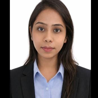
Abira Rashid
Materials Engineer
Gandhinagar
Work Preference
Summary
Materials Engineer specializing in ultra-high vacuum (UHV) thin-film systems, with extensive hands-on experience in PVD-based deposition and advanced characterization techniques, including SEM, TEM, and XRD. A robust background in integrating metrology with process development ensures controlled thickness, defect minimization, yield optimization, and reproducibility in thin films. Proficient in equipment operation, vacuum system management, SOP development, and root-cause troubleshooting, alongside expertise in foundry process design and optimization using PROCAST and DISA-based molding principles. Proven track record of developing innovative materials and enhancing manufacturing processes while demonstrating strong capabilities in materials testing and project management.
Overview
5
5
years of professional experience
Work History
Research Scholar (Prime Minister’s Research Fellow – PMRF) – Materials Engineering
IIT Gandhinagar
07.2021 - Current
- Developed UHV thin-film fabrication workflows integrated with post-deposition metrology, enabling thickness, defect density, and microstructure control with high reproducibility.
- Measured and interpreted thin-film properties (thickness, defects, phase, interfaces) using SEM, TEM, XRD, EBSD, and PED, linking metrology outputs to process parameters and performance.
- Designed and executed in-situ TEM/SEM experiments, generating and handling ~5 TB of high-resolution data for deformation and failure analysis.
- Tracked process and measurement consistency across batches using SPC; analyzed variability and implemented corrective actions to improve repeatability and system stability; applied structured parameter variation (DOE-approach) for process characterization and optimization.
- Evaluated process sensitivity to deposition parameters and identified critical process variables influencing film thickness, defect density, and microstructure.
- Executed chamber conditioning, bake-out procedures, deposition parameter tuning, and contamination control practices for consistent thin-film quality.
- Developed and maintained SOPs for SEM/TEM operation, calibration routines, and measurement workflows.
- Integrated process–structure–property correlation to diagnose deposition-induced defects and optimize film performance.
- Designed and fabricated free-standing thin films, requiring controlled deposition, handling, and process stability at nanoscale thickness.
- Designed and implemented an in-situ tensile testing methodology for pre-notched thin films, including experimental setup and instrumentation integration.
- Conducted root-cause analysis of failure mechanisms through in-situ TEM/SEM, linking defect evolution to processing conditions.
- Trained users on equipment operation, metrology practices, and contamination control.
- Maintained tool logs, monitored system performance, and supported troubleshooting of vacuum and microscopy systems to ensure high uptime and measurement reliability.
- Interacted with service engineers and vendors during maintenance and troubleshooting of UHV and microscopy systems.
- Collaborated across materials processing, advanced characterization, and data analysis teams to support application-oriented research.
- Application-Focused Projects:
- BN–SiO2 ceramics (Hall thrusters, ISRO): Microstructural and phase stability analysis using SEM, XRD, optical microscopy, and TGA for process–performance correlation
- Recycled Li-ion cathode materials: Phase evolution and microstructure assessment using SEM, XRD, and TGA to evaluate recycling-induced changes
- MOF growth on vapor-deposited films: Study of metal–organic framework growth on vapor-deposited thin films integrated with 2D membranes, focusing on interface-controlled growth and its application in ion separation.
- Tool wear and degradation: SEM-based microstructural analysis of worn tool surfaces to identify dominant wear mechanisms
- Epitaxial antiferromagnetic thin films (MnPtxPd1-x): Investigation of anisotropic magnetoresistance and structure–property relationships in epitaxial systems
- Quantum material (YbMnSb2) – ongoing work: HR-STEM analysis for defect (vacancy) identification and diffraction pattern simulation for structural interpretation
- Conducted comprehensive literature reviews to identify gaps in existing knowledge and inform future research directions.
- Optimized laboratory protocols and procedures ensuring stringent adherence to ethical guidelines while maintaining high-quality results.
- Developed new research methodologies that streamlined data collection processes, resulting in increased efficiency and accuracy of results.
Education
Ph.D. - Materials Engineering
Indian Institute of Technology, Gandhinagar
Gandhinagar, India 04.2001 -
M.Tech - Foundry and Forge Technology
NIFFT
Ranchi, India01-2021
B.Tech - Mechanical Engineering
FGIET
Raebareli, India01-2017
Skills
Thin-Film Deposition & Processing: PVD (sputtering/evaporation), thin-film growth kinetics, multilayer films, thickness control, deposition parameter optimization
UHV & Vacuum Systems: High-vacuum systems, pump operation (turbo/rotary), leak awareness, chamber conditioning, contamination control, basic vacuum troubleshooting
Characterization & Metrology: SEM, TEM, XRD, EBSD, EDS, PED, NDT, Defect and microstructure quantification
Measurement repeatability, calibration awareness, and error sources
Mechanical Failure & Fracture Characterization: Metallographic preparation (sectioning, mounting, grinding, polishing, etching), Tensile testing and deformation studies, Hardness testing (micro/macro), Tensile testing (In-situ SEM/TEM-based)
Process Control & Data Analysis: SOP/BKM development and revision; process variability analysis and repeatability tracking; SPC, DOE, and root cause analysis (RCA) for defect-driven and process-induced variations, process monitoring and optimization, process capability awareness (Cp/Cpk), process stability and reproducibility
Cleanroom & Handling: Thin-film handling, contamination mitigation, surface preparation, nanoscale specimen preparation
Foundry & Manufacturing: Casting design, gating and feeding optimization, PROCAST simulation, DISA process familiarity
Software & Data Analysis: ImageJ, Digital Micrograph, Origin, MATLAB, LAMMPS, ATAT, OVITO, Velox, SingleCrystal, Crystal Maker, ProCast, ANSYS
AWARDS AND RECOGNITIONS
Prime Minister’s Research Fellowship (PMRF) – Government of India (highly competitive national fellowship for doctoral research), Institute Rank 1 (First Position) – M.Tech, Foundry and Forge Technology, NIFFT Ranchi., First Prize- SPELLINC Competition.
PUBLICATIONS AND PRESENTATIONS
- Co-authored 9 peer-reviewed journal papers and 1 patent.
- Oral presentations: PTM-2025, EMSI 2024, NMD 2024, NMD 2023.
POSITIONS OF RESPONSIBILITY
- Graduate Teaching Fellow (GTF) – Microstructural Engineering, IIT Gandhinagar
- Teaching Assistant – TEM, SEM, Metallography Lab & Furnaces; IIT Gandhinagar, PDEU & Ahmedabad University
- Head Teaching Assistant – Wafer Characterization Laboratory (data curation, equipment coordination, user training, and lab management support)
Timeline
Research Scholar (Prime Minister’s Research Fellow – PMRF) – Materials Engineering
IIT Gandhinagar
07.2021 - Current
Ph.D. - Materials Engineering
Indian Institute of Technology, Gandhinagar
04.2001 -
B.Tech - Mechanical Engineering
FGIET
M.Tech - Foundry and Forge Technology
NIFFT