

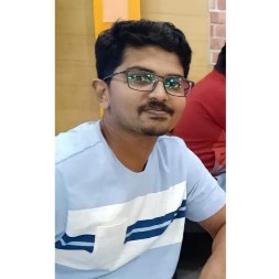
Sachin S
Bengaluru,IN
Overview
1
1
Certification
6
6
years of professional experience
Work History
Sr.Silicon design verification engineer
AMD
Bangalore, India
02.2026 - Current
Design verification engineer
Samsung Semiconductor India R&D
Bangalore, India
01.2021 - 02.2026
Intern
Samsung electronics
Bangalore, India
01.2021 - 06.2021
Intern
Indian Institute of Astrophysics
Bangalore, India
08.2020 - 12.2020
Education
B.Tech,Electronics and communication engineering
PES UNIVERSITY
Bangalore,India2021
Skills
- Design verification
- UVM
- Python scripting
- c programming
- Matlab and simulink system modeling
Professional summary
- Accumulated over 5 years of experience in writing testbenches in SV and UVM
- Worked at Samsung R&D,south korea for an year for RTL architecture discussions and fast forward verification
- Working at AMD on custom asic verification at subsystem level
- Specialised in IP verification of memory controllers-UFS using SV,UVM
- Testing and implementing scenrios for verifying the functionality of their design
- Developed expertise in AXI and AHB protocols.
- Planned and implemented automated testing scripts with python, minimising manual work in testingand maximising team performance.
- Worked with Agile and Scrum methodologies to accomplish project milestones and meet demanding timelines.
- Logged findings in detail following standard procedures for optimum collaboration across technical team.
- Documented, triaged and managed defects in JIRA and worked with developers to facilitate timely resolutions.
- Completed unit and regression tests on individual modules.
PROJECT DETAILS
- VERIFICATION OF CUSTOM BEAMFORMER ASIC
DESCRIPTION: This is a custom asic performing tranceiver functions and analog front end supporting 32 transmit and receive antennas.The subsytem verified handles clock generaton,reset,boot and debug functions.
RESPONSIBITLITIES:
1. Developed Checkers for noc inside cpu subsystem
2. Debug interfaces end to end verififcaion-JTAG
3. IP verification(acts like a buffer) end to end verification including coverage
- VERIFICATION OF UFS DEVICE IP->UTP
DESCRIPTION: Universal Flash Storage is a flash storage specification for mobile phones and consumer electronic devices and has a layered structure for data propogation.UTP(UFS transport protocol) is an IP that handles command reception from the HOST,processes and does DMA operations.
RESPONSIBITLITIES:
1. Developed Checkers for write and read DMA
2. Interrupt and interrupt mask tcs and checker
3. Error scenerio handling checkers
- VERIFICATION OF UFS DEVICE IP->HCP
DESCRIPTION: HCP is a HOST command processor IP that handles the scheduling/throttling of cmds before doing the flash operations.It was included to accelerate the hardware performance by offloading firmware tasks to this IP.
RESPONSIBITLITIES:
1. Developed VPlan and Checker plan and had architecture discussions during the initial phase of the project.
2. Developed the uvm tb components and sequences from the scratch,including testbench models.
3. End to end functional verification,coverage was executed
VERIFICATION OF UFS DEVICE IP->HTH
DESCRIPTION: HTH is a HOST task handler that handles the processing of descriptors before dma operations by UTP.
RESPONSIBITLITIES:
1. Checkers independent of the existing architecture was created
2. coverage during constrainted schedule was executed.
DEVELOPEMENT OF DEBUGGING SCRIPTS AND GUI FOR VERIFCATION
1.Python script to extract data from the hang/error logs to identify the issue fast forward for new joinees.
2.Perl script rearchitecture for debugging datapath of UTP IP
Additional Information
1)High altitude research balloon project.(Stabilisation model with pid) This project involves payload with experiments(stabilisation,solar flux density)
https://docs.google.com/presentation/d/1sCd4w2F3UeHljDz9uCwbT3mGQRF02S52rLe an7lJJnQ/edit?usp=sharing
2)Gesture recognition
3)3D mapped delivery system
4)Smart traffic detection - Image processing(RCNN),Geo position based alerting https://drive.google.com/drive/folders/12-ltKSnnFWdPs3xxVg_E17nk6c8mvkIg?usp=sharing
5)Development of LVDT amplifier
6)Automatic water reader
https://docs.google.com/presentation/d/1MWmgQ2QowwGFiJZd1wd3bgV3zPeOGQeveT6Dvio p2os/edit?usp=sharing
Accomplishments
- Multiple Employee of the Month awards
- 4 CNRR scholarship from PES UNIVERSITY(Top 20% of the batch
- 1st prize in STEP technology and policy(IIT Madras,2020
- 1st prize in microcontroller programming(Shaastra,IIT Madras,2020) https://drive.google.com/file/d/1jY2gaOp0bWTuNVtpMQVtqOlLoj3YNuDy/view?usp=sharing
Certification
- Universal Verification Methodology - UVM
- System verilog for verification
Timeline
Sr.Silicon design verification engineer
AMD
02.2026 - Current
Design verification engineer
Samsung Semiconductor India R&D
01.2021 - 02.2026
Intern
Samsung electronics
01.2021 - 06.2021
Intern
Indian Institute of Astrophysics
08.2020 - 12.2020
B.Tech,Electronics and communication engineering
PES UNIVERSITY